555 Timer Applications: Astable Oscillators and PWM
In astable mode, the 555 has no stable resting state. It repeatedly charges and discharges a timing capacitor, producing a square wave on the output pin. This makes it useful for LED flashers, beepers, clocks, alarms, pulse-width modulation, and simple test signals.
Learning Objectives
By the end of this lesson, you should be able to wire a 555 astable, calculate high time, low time, frequency, and duty cycle, explain why the standard circuit is above 50% duty cycle, and troubleshoot common oscillator problems.
Astable Circuit
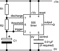
Typical connections:
R1fromVccto pin 7.R2from pin 7 to pins 2 and 6.Cfrom pins 2 and 6 to ground.- Pin 4 tied high.
- Pin 5 bypassed to ground with
10 nF. - Pin 3 is the square-wave output.
Pins 2 and 6 are tied together so the timing capacitor retriggers the IC automatically.
How the Oscillation Works
- Output high: pin 7 is off and the capacitor charges through
R1 + R2. - At
2/3 Vcc: threshold comparator resets the latch and output goes low. - Output low: pin 7 turns on and the capacitor discharges through
R2. - At
1/3 Vcc: trigger comparator sets the latch and output goes high again.
The capacitor voltage is an exponential waveform between 1/3 Vcc and 2/3 Vcc; the output is a square wave.
title "Ideal 555 astable timing"
time start=0 end=4 unit=ms divisions=8
OUT: square label="Output" low=0 high=5 duty=60 cycles=2 unit=V color=#2563eb
VCAP: triangle label="Timing capacitor" min=1.67 max=3.33 cycles=2 unit=V color=#16a34a
marker UPPER at=1.2 label="2/3 Vcc"
marker LOWER at=2.0 label="1/3 Vcc"
The waveform is explanatory; it is not a SPICE simulation and does not include real output rise time or capacitor exponential curvature.
Timing Formulas
$$
T_{HIGH} = 0.693(R_1 + R_2)C
$$
$$
T_{LOW} = 0.693R_2C
$$
$$
T = T_{HIGH} + T_{LOW} = 0.693(R_1 + 2R_2)C
$$
$$
f = \frac{1}{T} \approx \frac{1.44}{(R_1 + 2R_2)C}
$$
$$
D = \frac{T_{HIGH}}{T} = \frac{R_1 + R_2}{R_1 + 2R_2}
$$
In the standard astable circuit, duty cycle is always greater than 50% because charging uses R1 + R2, while discharging uses only R2.
Try It: 555 Astable Calculator
Enter `R1`, `R2`, and either capacitance or frequency.
Formulas: `f = 1.44 / ((R1 + 2R2) C)` and `D = (R1 + R2) / (R1 + 2R2)`.
Worked Example: 1 Hz LED Flasher
Goal: blink near 1 Hz.
Choose R1 = 1 kOhm, R2 = 68 kOhm, and solve for C:
$$
C = \frac{1.44}{f(R_1 + 2R_2)}
= \frac{1.44}{1(1000 + 2 \times 68000)}
= 10.5 \mu F
$$
Use 10 uF.
Check:
$$
T_{HIGH} = 0.693(1k + 68k)(10uF) = 0.478 s
$$
$$
T_{LOW} = 0.693(68k)(10uF) = 0.471 s
$$
The blink rate is about 1.05 Hz, close enough for an indicator.
Worked Example: 1 kHz Tone
Goal: generate an audio tone near 1 kHz.
Choose C = 100 nF and R1 = 1 kOhm.
$$
R_1 + 2R_2 = \frac{1.44}{1000 \times 100 nF} = 14.4 k\Omega
$$
$$
R_2 = \frac{14.4 k\Omega - 1 k\Omega}{2} = 6.7 k\Omega
$$
Use 6.8 kOhm. Drive a piezo directly if allowed by its datasheet; use a transistor or amplifier for heavier speakers.
Variable Frequency and Duty Cycle
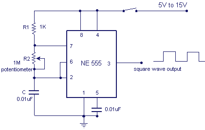
Replacing R2 with a potentiometer changes both frequency and duty cycle. Add a fixed resistor in series so the resistance never reaches zero.
For closer to 50% duty cycle, add steering diodes so the capacitor charges through one resistance and discharges through another.
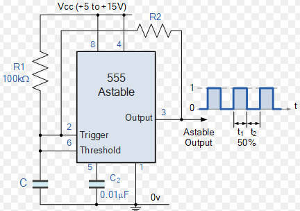
With the diode steering method:
$$
T_{HIGH} \approx 0.693R_{charge}C
$$
$$
T_{LOW} \approx 0.693R_{discharge}C
$$
Use matched resistors for a near-50% duty cycle.
PWM Applications
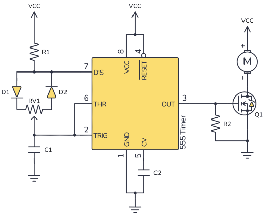
PWM controls average power by changing duty cycle while keeping switching frequency high enough for the load.
Common uses:
- LED dimming above visible flicker frequency, often above
200 Hz; - small DC motor speed control through a transistor or MOSFET;
- heater power control with proper isolation and protection;
- audio tone and siren effects.
Do not drive motors, relays, or high-current LEDs directly from pin 3 unless the current is within the selected 555 variant rating. Use a transistor or MOSFET driver and a flyback diode for inductive loads.
Practical Frequency Ranges
0.1 Hzto10 Hz: indicators, alarms, slow timing; leakage matters.10 Hzto1 kHz: low-frequency control and audible effects.1 kHzto100 kHz: tones, clocks, PWM.- Above
100 kHz: use CMOS 555 parts or dedicated oscillators; layout and propagation delay become important.
Troubleshooting
- No oscillation: check pins 2 and 6 are tied, reset pin 4 is high, and capacitor returns to ground.
- Output stuck high: pin 7 may be open, capacitor may not reach
2/3 Vcc, or discharge path is wrong. - Output stuck low: reset may be low or trigger node may be shorted.
- Wrong frequency: measure actual capacitor value and resistor values.
- Unstable frequency: improve supply decoupling and use stable capacitors.
- Load distorts output: buffer pin 3 with a transistor or logic gate.
Summary
The 555 astable converts an RC charge-discharge cycle into a continuous square wave. The key formulas are THIGH = 0.693(R1 + R2)C, TLOW = 0.693R2C, and f = 1.44 / ((R1 + 2R2)C). Practical designs need reset wiring, control-pin bypassing, supply decoupling, minimum resistance limits, and a proper output driver for real loads.
Further Reading
- Texas Instruments, NE555 and TLC555 datasheets.
- STMicroelectronics, "TS555 Low Power Single CMOS Timer."
- Forrest Mims, Timer, Op Amp, and Optoelectronic Circuits and Projects.
- Manufacturer application notes on 555 PWM and astable operation.